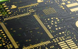
HDI microvia pcb
our printed circuit PCB HDI Mivrovia
 PCB layout design designs printed circuit boards, wiring and pad density than conventional PCBs, with widths and smaller traces spaces.They require advanced PCB technologies such as blind vias, buried vias and microvias. HDI PCB Mivrovia are generally more expensive than conventional PCB because of the complex accumulation process involved in manufacturing.
Pourquoi opter pour la technique Microvia ?
The PCB HDI (High Density Interconnection) and microvia technology are inseparable. The microvia technology ensures, through the smallest holes made by laser, electrical connection between the layers of a multilayer board.
As part of the miniaturization of PCBs, microvias "via-in-pad" play a decisive role. "Via in Pad" means that microvia holes are positioned directly in the solder pads. Since microvias constitute no blind holes, there is no capillary effect. The solder deposit fills the minimum hollow.
Cette méthode offre de nombreux avantages :
- Possibilité de layout avec BGA à faible entraxe
- Miniaturisation grâce à la technique "Via in pad"
- Obtention à faibles coûts d'un réseau de câblage très dense
- Technique pérenne – car les composants futurs seront de plus en plus petits
- Fiabilité optimale
- Réduction d'effets parasites au niveau des inductances et de la capacité
Our specific technologies:
- HDI Printed-circuit boards (High Density Interconnect)
 Via in pad (capped via)
- µvia Copper Filling
- Via plugged with non-conductive paste, copper, solder masks or via filler SD-2361 "Peters"
- Stacked µvia
- LDI - LPI and horizontal metalisation for complex products
- Clean room class 1,000/10,000/100,000 for complex boards
- Possibility of using different substrates on the same board through "laser adjustment" technology of our press
Certifications and Standards: UL, ISO 9001 :2008, ISO 14001 :2004, IPC class 1,2 and 3, ROHS, REACH, others on request...
